www.vishay.com
119
1401
Vishay Foil Resistors
Document Number: 63037
Revision 31-Jul-02
THROUGH HOLE
VISHAY FOIL • FRANCE +33.4.93.37.28.24 FAX: +33.4.93.37.27.31
• GERMANY +49.9287.710 FAX: +49 9287.70435
• ISRAEL +972.3.557.0945 FAX: +972.3.558.9121
• ITALY + 39.2.300.11919 FAX: +39.2.300.11999
• JAPAN +81.42.729.0661 FAX: +81.42.729.3400
• SINGAPORE +65.788.6668 FAX: +65.788.0988
• SWEDEN +46.8.594.70590 FAX: +46.8.594.70581
• UK +44 191 514 8237 FAX: +44 1953 457 722
• USA +1 610 407-4800 FAX: +1 610 640-9081
Bulk Metal
®
Foil Technology
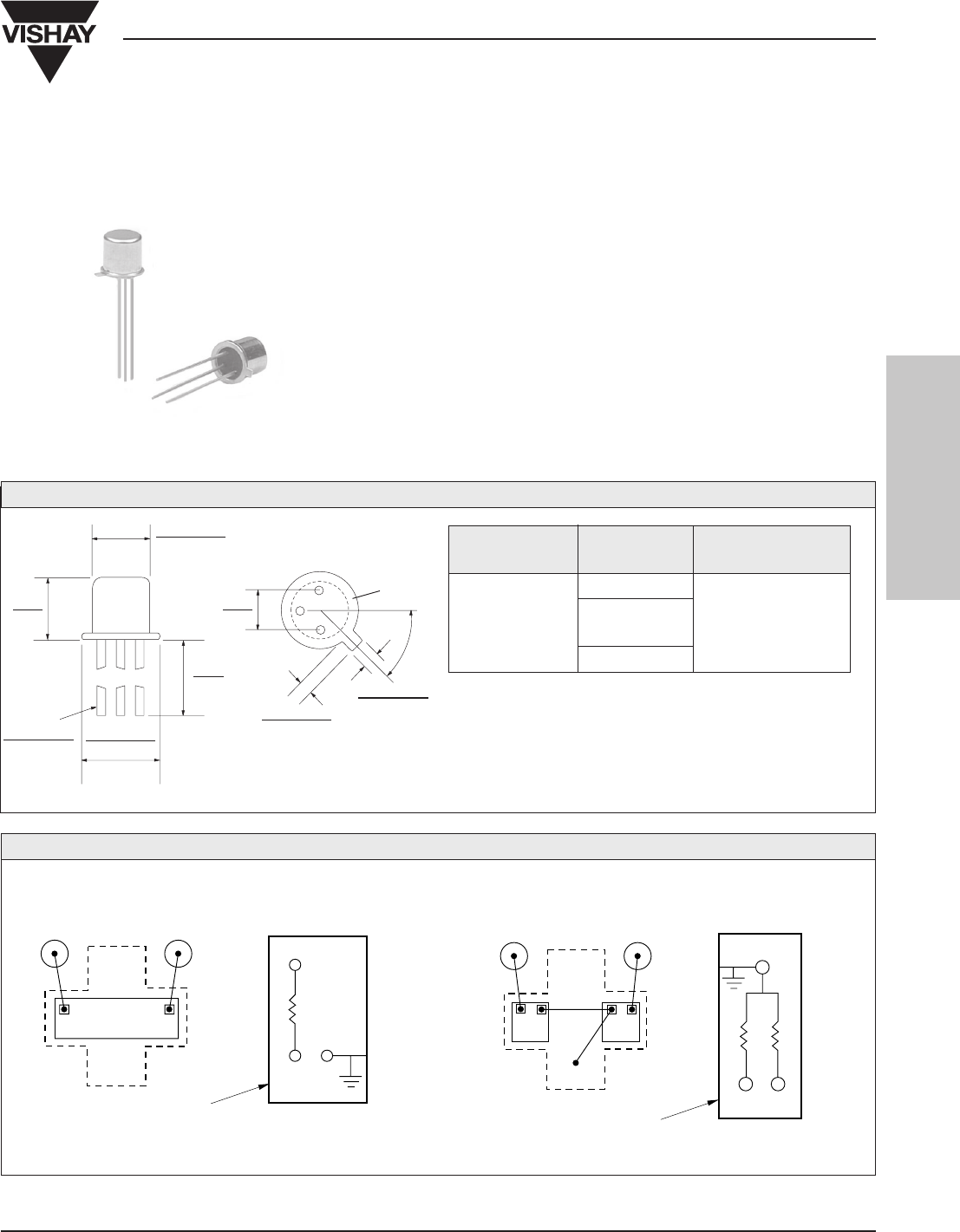
3 Pin Transistor Outline Hermetic Resistor Network
The three pin TO-18 package is suitable for single resistor
hermetic packaging with case and lid grounded for electrical
isolation. This unique package may also be used to provide a
voltage divider, but the user is cautioned that the center tap must
go to ground.
Review data sheet “7 Technical Reasons to Specify Bulk
Metal
®
Foil Resistor Networks.”
3 pins on a 0.100" pin circle– pin 3 case grounded.
FIGURE 1 - STANDARD DIMENSIONS in inches (millimeters)
ORDERING INFORMATION - 1401 PARTS
Networks are built to your requirements. Send your schematic
and electrical requirements to the Applications Engineering
Department. (See data sheet “Network Worksheet.”) A unique
part number will be assigned which defines all aspects of your
network.
VISHAY CHIP
MAXIMUM POWER RATING
MODEL NUMBER CAPACITY (WATTS) @ +70°C
V15X5 - 1 chip
V15X5 - 1 chip
1401 and 0.15 Watt
V5X5 - 1 chip
V5X5 - 2 chips
0.036 –0.046
(0.91 –1.17)
DIAMETER
0.178 –0.195
(4.52 –4.95)
0.500
(12.7)
0.209 –0.230
(5.31 –5.84)
DIAMETER
MAXIMUM
0.200
(5.08)
0.016 –0.021
(0.41 –0.48)
3 LEADS
2
3
1
0.028 –0.048
(0.71 –1.22)
0.100
(2.54)
CASE
GROUNDED
45°
NOTES:
1. These networks utilize Vishay Bulk Metal
®
Foil resistor
chips V5X5 and V15X5 or VTF15X10 Thin Film chips.
2. The V5X5 and V15X5 chips have maximum resistance
values of 10K and 33K respectively in Bulk Metal
®
Foil
and 500K in VTF15X5 Thin Film chips.
FIGURE 2 - SAMPLE CIRCUIT DESIGNS AND CHIP LAYOUTS
NOTE: Usable area is represented by the dotted lines— a cross 0.150 Inches x 0.150 Inches with arm width of 0.05 Inches.
Illustrations not to scale. Chips shown undersize for clarity. Drawing view is from the top looking down into the
package.
R1
21
R1
R1
2
3
CASE
CASE
ONE RESISTOR
CASE GROUNDED
DIVIDER
CENTER TAP GROUNDED
1
2
R2
3
2
1
R1
R2
3
(VIEWED FROM BOTTOM)
Product may not
be to scale
MINIMUM