Integrated Device Technology, Inc.
The IDT logo is a registered trademark of Integrated Device Technology, Inc.
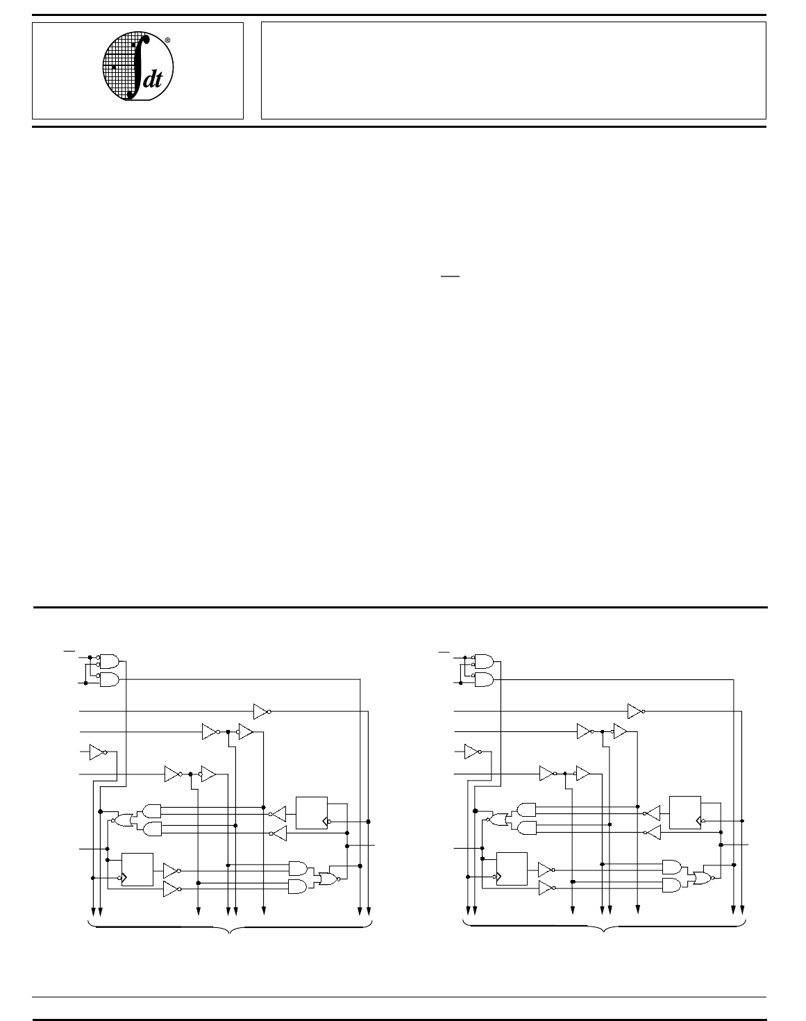
FUNCTIONAL BLOCK DIAGRAM
FAST CMOS 16-BIT BUS
TRANSCEIVER/
REGISTERS (3-STATE)
IDT54/74FCT16646T/AT/CT/ET
IDT54/74FCT162646T/AT/CT/ET
1B1
1
A1
1
OE
1DIR
1SBA
1SAB
1CLKBA
1CLKAB
2540 drw 01
TO 7 OTHER CHANNELS
B REG
A REG
D
C
C
D
2
A
1
2
OE
2
DIR
2
SBA
2
SAB
2
B
1
2
CLKBA
2
CLKAB
2540 drw 02
TO 7 OTHER CHANNELS
B REG
A REG
D
C
C
D
74FCT162646T/AT/CT/ET 16-bit registered transceivers are
built using advanced dual metal CMOS technology. These
high-speed, low-power devices are organized as two inde-
pendent 8-bit bus transceivers with 3-state D-type registers.
The control circuitry is organized for multiplexed transmission
of data between A bus and B bus either directly or from the
internal storage registers. Each 8-bit transceiver/register fea-
tures direction control (xDIR), over-riding Output Enable con-
trol (x ) and Select lines (xSAB and xSBA) to select either
real-time data or stored data. Separate clock inputs are
provided for A and B port registers. Data on the A or B data
bus, or both, can be stored in the internal registers by the
LOW-to-HIGH transitions at the appropriate clock pins. Flow-
through organization of signal pins simplifies layout. All inputs
are designed with hysteresis for improved noise margin.
The IDT54/74FCT16646T/AT/CT/ET are ideally suited for
driving high-capacitance loads and low-impedance
backplanes. The output buffers are designed with power off
disable capability to allow "live insertion" of boards when used
as backplane drivers.
The IDT54/74FCT162646T/AT/CT/ET have balanced
output drive with current limiting resistors. This offers low
ground bounce, minimal undershoot, and controlled output
fall times–reducing the need for external series terminating
resistors. The IDT54/74FCT162646T/AT/CT/ET are plug-in
replacements for the IDT54/74FCT16646T/AT/CT/ET and
54/74ABT16646 for on-board bus interface applications.
MILITARY AND COMMERCIAL TEMPERATURE RANGES AUGUST 1996
1996 Integrated Device Technology, Inc. 5.13 DSC-4231/9
1
DESCRIPTION:
The IDT54/74FCT16646T/AT/CT/ET and IDT54/
FEATURES:
• Common features:
– 0.5 MICRON CMOS Technology
– High-speed, low-power CMOS replacement for
ABT functions
– Typical tSK(o) (Output Skew) < 250ps
– Low input and output leakage ≤1µA (max.)
– ESD > 2000V per MIL-STD-883, Method 3015;
> 200V using machine model (C = 200pF, R = 0)
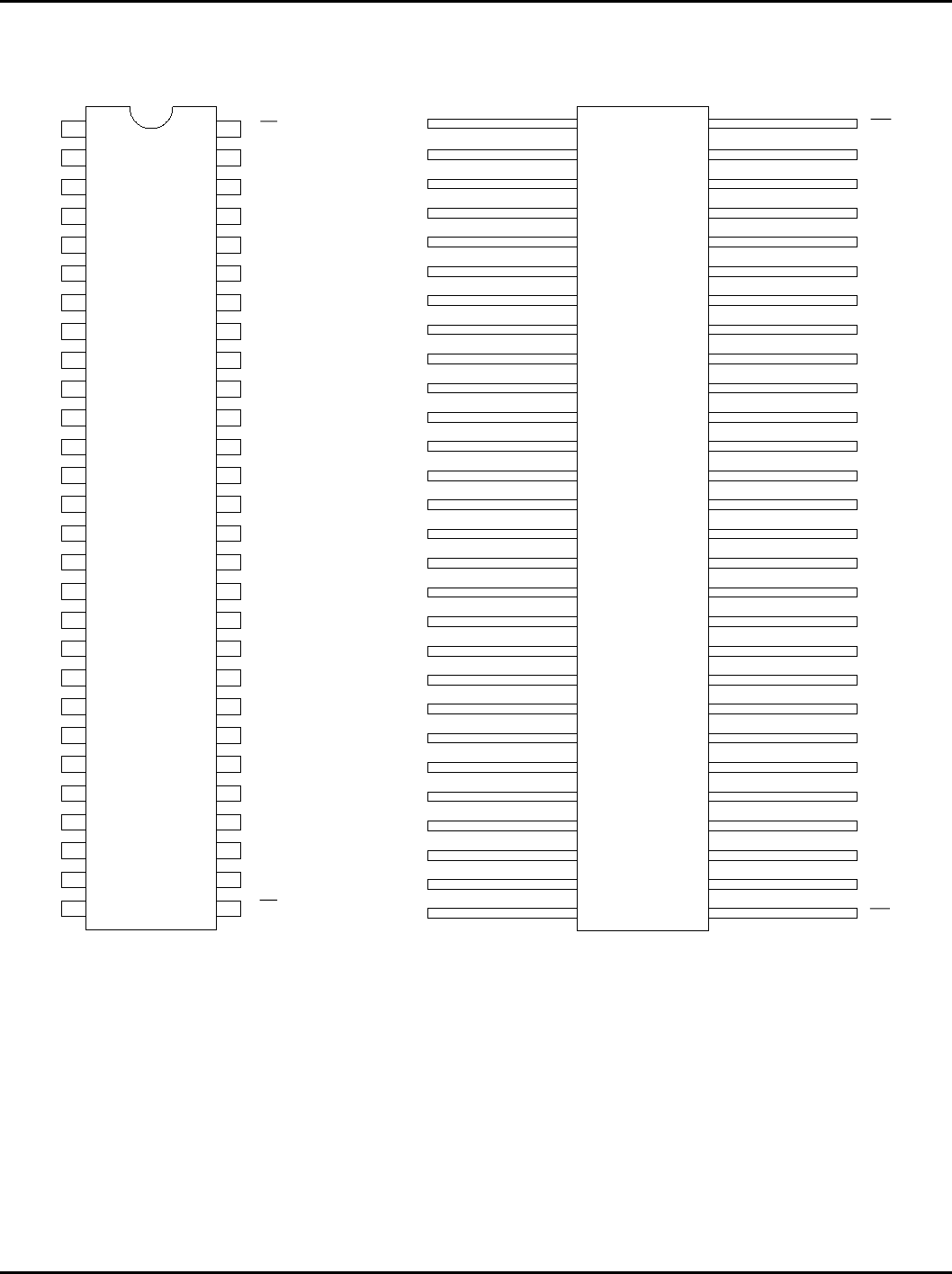
– Packages include 25 mil pitch SSOP, 19.6 mil pitch
TSSOP, 15.7 mil pitch TVSOP and 25 mil pitch Cerpack
– Extended commercial range of -40°C to +85°C
–VCC = 5V ±10%
• Features for FCT16646T/AT/CT/ET:
– High drive outputs (-32mA IOH, 64mA IOL)
– Power off disable outputs permit “live insertion”
– Typical VOLP (Output Ground Bounce) < 1.0V at
VCC = 5V, TA = 25°C
• Features for FCT162646T/AT/CT/ET:
– Balanced Output Drivers: ±24mA (commercial),
±16mA (military)
– Reduced system switching noise
– Typical V
OLP (Output Ground Bounce) < 0.6V at
VCC = 5V,TA = 25°C
IDT54/74FCT16646T/AT/CT/ET, 162646T/AT/CT/ET
FAST CMOS 16-BIT BUS TRANSCEIVER/REGISTER MILITARY AND COMMERCIAL TEMPERATURE RANGES
5.13 3
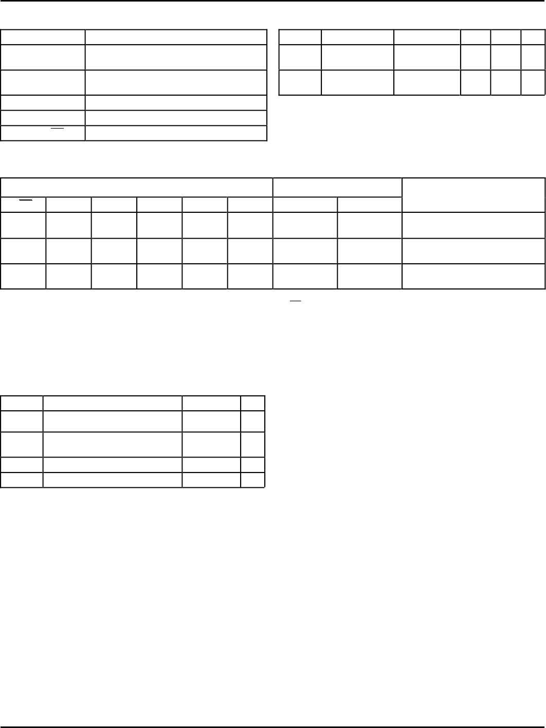
PIN DESCRIPTION
FUNCTION TABLE
(2)
CAPACITANCE (TA = +25°C, f = 1.0MHz)
2540 tbl 01
NOTE:
1. This parameter is measured at characterization but not tested.
2540 tbl 02
NOTES: 2540 tbl 03
1. The data output functions may be enabled or disabled by various signals at the x or xDIR inputs. Data
input functions are always enabled, i.e. data at the bus pins will be stored on every LOW-to-HIGH transition
on the clock inputs.
2. H = HIGH Voltage Level
L = LOW Voltage Level
X = Don't Care
↑ = LOW-to-HIGH Transition
ABSOLUTE MAXIMUM RATINGS
(1)
Symbol Parameter
(1)
Conditions Typ. Max. Unit
CIN Input
Capacitance
VIN = 0V 3.5 6.0 pF
CI/O I/O
Capacitance
VOUT = 0V 3.5 8.0 pF
Pin Names Description
xAx Data Register A Inputs
Data Register B Outputs
xBx Data Register B Inputs
Data Register A Outputs
xCLKAB, xCLKBA Clock Pulse Inputs
xSAB, xSBA Output Data Source Select Inputs
xDIR, x Output Enable Inputs
Inputs Data I/O
(1)
Operation or Function
x xDIR xCLKAB xCLKBA xSAB xSBA xAx xBx
H
H
X
X
H or L
↑
H or L
↑
X
X
X
X
Input Input Isolation
Store A and B Data
L
L
L
L
X
X
X
H or L
X
X
L
H
Output Input Real Time B Data to A Bus
Stored B Data to A Bus
L
L
H
H
X
H or L
X
X
L
H
X
X
Input Output Real Time A Data to B Bus
Stored A Data to B Bus
Symbol Description Max. Unit
VTERM
(2)
Terminal Voltage with Respect to
GND
–0.5 to +7.0 V
VTERM
(3)
Terminal Voltage with Respect to
GND
–0.5 to
V
CC +0.5
V
TSTG Storage Temperature –65 to +150 °C
IOUT DC Output Current –60 to +120 mA
2540 tbl 04
NOTES:
1. Stresses greater than those listed under ABSOLUTE MAXIMUM RAT-
INGS may cause permanent damage to the device. This is a stress rating
only and functional operation of the device at these or any other conditions
above those indicated in the operational sections of this specification is not
implied. Exposure to absolute maximum rating conditions for extended
periods may affect reliability.
2. All device terminals except FCT162XXXT Output and I/O terminals.
3. Output and I/O terminals for FCT162XXXT.